From Fundamental Research to Industrial Application
With academic customers around the globe, Exaddon has established itself provider of pioneering 3D printing technology to research teams at the cutting edge of science.
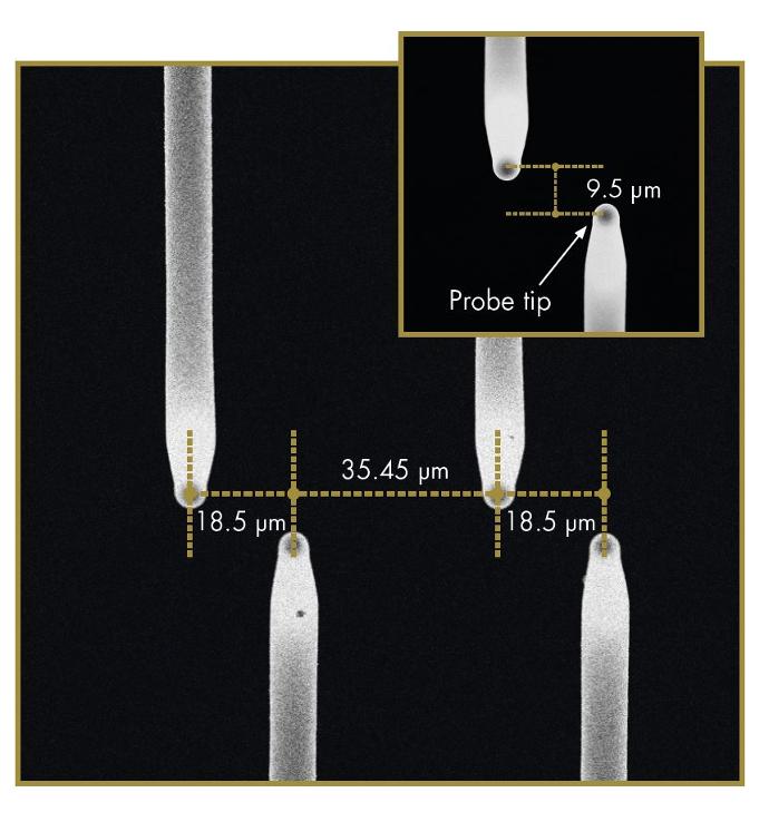
In the past two years, Exaddon has developed an industrial solution; 3D microprinting of probes for fine-pitch probing at sub 20 μm pitch.
Disrupting Semiconductor Wafer Testing with 3D Printing

Semiconductors are the real building blocks of modern-day life, powering our devices, transport, and communications.
Amongst the most secretive and high-tech industries in the world, the $500bn semiconductor industry [1] depends on a complex and demanding process to ensure that defect-free dies make it into packaged components; wafer probing.
Despite all the innovation and resources available, the wafer probing industry is struggling to reach pitches below 40 μm, limiting chip design and the continued scaling necessary to keep up with consumer demand.
Nowhere is this more apparent than in microLEDs.
With an 80% CAGR and a valuation at tens of billions (USD) in the next 5 years [2], the microLED market is waiting to explode, yet testing lags far behind, with LEDs being tested individually by two-probe setups.
What’s the solution?
Enter Exaddon and Microscale 3D Printing

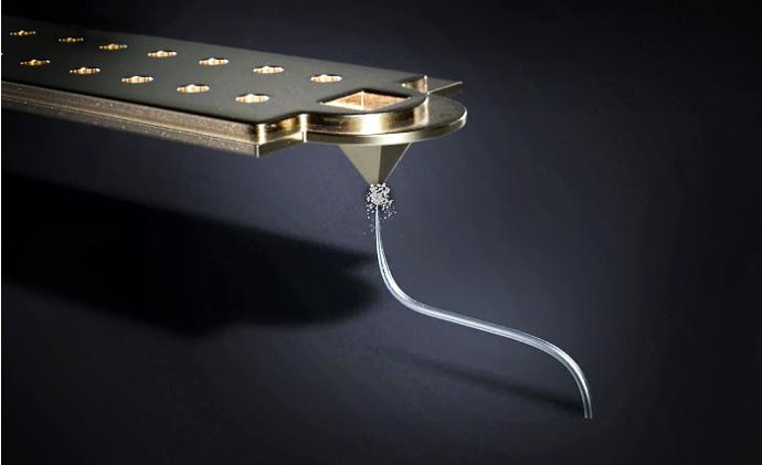
3D printing microscale structures in complex geometries is exactly where Exaddon’s micro3D printing technology excels, delivering high quality printed metal with micrometer resolution.
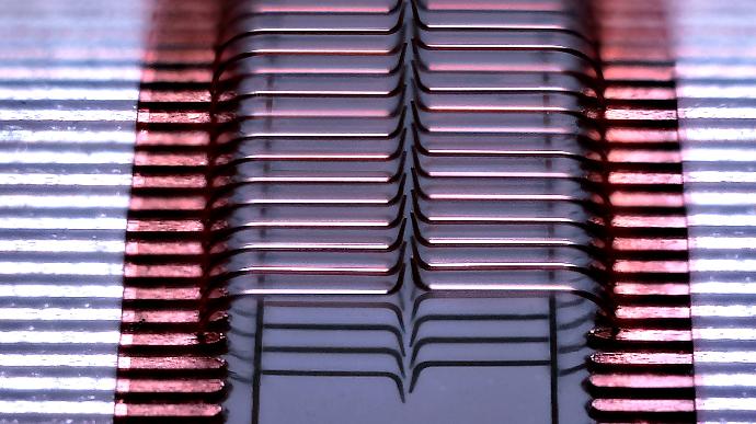
Exaddon’s initial microLED test array is 3D printed directly on prepatterned traces with a pitch of less than 20 μm; under half the current industry limit.
This demonstrator validates Exaddon’s process on microPCBs for mounting on current probe heads. With 128 probes, the array gives microLED testers a 64x increase in efficiency.
Exaddon’s process also simplifies probe manufacturing by printing directly on customizable and exchangeable space transformers; cutting out layers of components, complexity, and cost.
Increase Active Die Area and Yield

The potential benefits are huge. Testing at finer pitch enables greater active die area, thus increasing yield and reducing chip cost, ultimately reducing consumer device cost.
The template-free 3D printing process is highly customizable and excels at printing high aspect ratio, freestanding structures. Various pad/bump/ball structures can be contacted.
The unique capabilities of Exaddon’s micro3D printing technology, made possible by local electrodeposition of pure metal, offers an unprecedented route toward successfully accessing and testing at sub 20 μm pitch.
Any application which requires fine pitch probing below the current pitch limit stands to benefit from this unique approach.
Discover Exaddon Wafer Probing
References:
[1] https://www.wsts.org/esraCMS/extension/media/f/WST/6032/WSTS_nr-2023_05.pdf
[2] https://www.giiresearch.com/report/marf1063219-micro-led-display-market-forecast-till.html
Beyond Fine Pitch: Exaddon Probe Testing Now Live